Navigate this guide · 1,620 words
The essential signal
- The ideal continuous-conduction voltage ratio is a starting model, not a universal operating rule.
- Inductor peak current includes ripple as well as the load current.
- Use the converter data sheet for component ranges, limits and compensation requirements.
A lower output needs an energy path
A buck converter is easier to understand when you follow the current rather than imagine a device simply throwing away excess voltage. Its power stage switches the input connection and uses an inductor and capacitors to support a lower output. Texas Instruments' power-stage note considers converters operating in continuous conduction, where the inductor current stays above zero throughout the switching cycle. That qualification matters: equations derived for this mode should not be treated as a complete description of every light-load operating mode.[1]
Start with four practical questions: what input range is available, what output voltage is needed, how much output current must be supplied, and which converter IC is under consideration? TI uses those inputs to organize its calculations. The last question cannot be postponed indefinitely because the IC determines switching limits and recommended component ranges. This article explains the relationships in that calculation, not a construction procedure for mains equipment or a claim that a generic circuit will be safe for a particular load.[1]

What the ideal duty ratio actually says
In the ideal steady-state continuous-conduction model, the output-to-input voltage ratio equals the switch duty cycle. Duty cycle is the fraction of each switching period for which the high-side switch conducts. The relationship follows from balancing the inductor's average voltage over a complete cycle. It gives a useful mental picture: changing the balance between the two switching intervals changes the operating point. It does not remove semiconductor losses, timing restrictions or the need to verify that the assumed operating mode applies.[1]
For a hypothetical 12-volt input and 5-volt output, the ideal ratio is about 0.417. That is an explanatory calculation, not a recommended controller setting. TI's practical calculation also accounts for efficiency when estimating duty cycle. Real parts have minimum on-times, operating limits and control behavior documented by their manufacturers. Keep the ideal ratio beside those details rather than replacing them with it. A neat result from a calculator is useful only when the selected device can operate under the conditions used to obtain it.[1]
The inductor current rises and falls
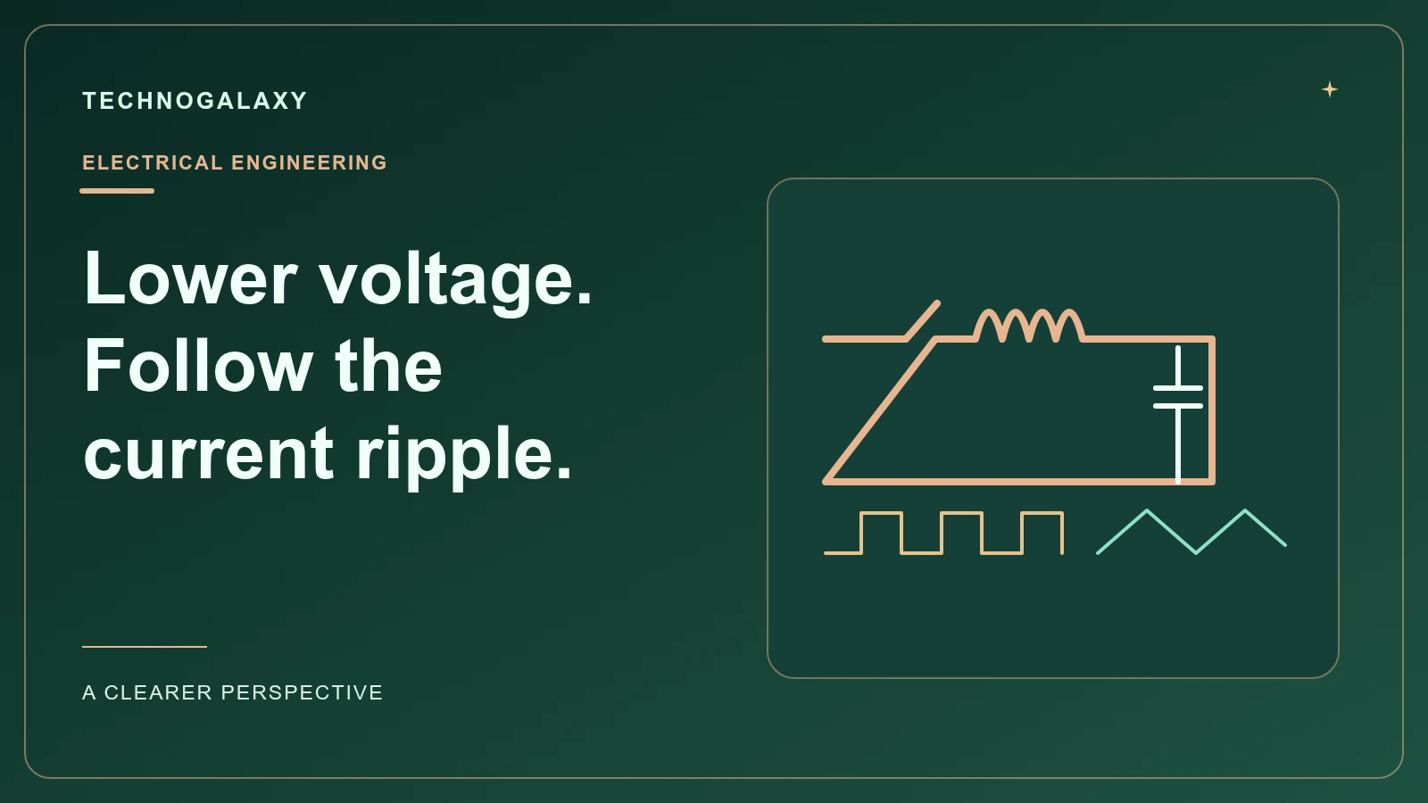
During the interval when the input drives the inductor toward the output, the voltage across the inductor causes its current to rise. During the other interval, the current continues through the available freewheeling path and falls. A diode supplies that path in the basic asynchronous arrangement shown by TI; a second controlled switch replaces it in a synchronous converter. Those are different implementations of the switching path, not permission to interchange component-loss calculations without checking the topology.[1]
The resulting ripple sits on top of the average current needed by the load. Under the assumed continuous-conduction conditions, the average inductor current supplies the output, while the peak is higher. That is why a current rating cannot be selected from the load's average demand alone. Draw the current waveform with a marked average, minimum and maximum before choosing parts. The sketch immediately makes visible a requirement that can disappear when a design is summarized only as an output voltage and an ampere rating.[1]

Peak current is a separate requirement
TI calculates application peak switch current by adding half the peak-to-peak inductor ripple to the maximum output current. For example, a hypothetical 2-ampere load with 0.6 ampere of peak-to-peak ripple produces a 2.3-ampere peak in this simplified calculation. The arithmetic is straightforward, but the distinction is important: average load current and peak component current answer different questions. Label both numbers so that a later component substitution does not silently discard the ripple allowance.[1]
The note also checks the converter's minimum specified current limit rather than assuming every unit reaches a favorable typical value. Inductors, switches and the rectifying path must be considered against the relevant current requirements. This is not a complete thermal or fault analysis; it is one necessary part of selecting a workable power stage. If the calculation leaves no room within the documented device limits, revisit the selection instead of describing a marginal result as acceptable because the average current appears small enough.[1]
Inductance changes the ripple trade-off
For otherwise comparable continuous-conduction conditions, increasing inductance reduces current ripple. TI recommends starting with the inductor range in the converter data sheet where one is provided. That advice keeps the calculation tied to the controller the manufacturer actually characterized. Choosing a value far outside the recommended range merely because it makes one equation attractive can ignore the converter's operating requirements. The objective is a compatible design, not the smallest ripple number that can be produced on paper.[1]
A smaller inductor can help reduce physical size, but the selection still has to satisfy peak-current requirements. TI explicitly warns that current rises as inductance decreases. In a design worksheet, keep inductance, ripple and current rating in adjacent columns. This makes the trade-off easier to review and helps prevent an attractive package size from becoming the only selection criterion. The worksheet should also identify the exact component and its documented limits rather than treating every part carrying the same nominal inductance as interchangeable.[1]
Output ripple has more than one contributor
The output capacitor helps accommodate the difference between the changing inductor current and the load's demand. TI separates a capacitance-related ripple contribution from an additional contribution associated with equivalent series resistance, or ESR. The point is not that one capacitor specification predicts the entire output waveform. It is that both stored charge and nonideal resistance belong in the explanation. A capacitance value printed on a component list therefore needs the accompanying part characteristics and the operating assumptions used in the calculation.[1]
Steady-state ripple is only one requirement. TI notes that load-transient behavior often drives output-capacitor selection because inductor current cannot immediately match a changed load demand. An output that looks satisfactory under a constant load may behave differently during a step. A useful review separates those two cases: repetitive ripple during established operation, and voltage deviation while current catches up after a change. Neither should be represented by a single unlabeled screenshot or by a result obtained under unspecified loading conditions.[1]

The input capacitor has a job too
It is tempting to focus entirely on the output, but a switching converter also asks its input supply to deliver a changing current. TI identifies the input capacitor as necessary for supporting the peak-current demand and stabilizing the local input voltage. The selected IC's data sheet normally provides a minimum value. Treat that requirement as part of the power-stage design rather than an optional accessory added after the converter has already been chosen and the board arrangement has been fixed.[1]
TI discusses low-ESR ceramic capacitors and suitable dielectric behavior because usable capacitance depends on operating conditions. The nominal number alone does not settle the selection. For an engineering comparison, record the actual capacitor family and the conditions under which its capacitance is specified. This does not mean every capacitor needs to be oversized without reason. It means the value used in the calculation should correspond to the component's relevant behavior, rather than to a label separated from voltage, temperature and the manufacturer's supporting information.[1]
Feedback sets a target, not unlimited ability
Many adjustable converters sense a fraction of the output through a resistor divider. The controller compares that feedback signal with its reference and adjusts operation accordingly. TI's divider calculation accounts for feedback-pin bias current so the sensing network does not create an overlooked error. This is another reason to use the selected IC's documentation: the feedback voltage and bias-current assumptions belong to the device, not to a universal buck-converter symbol that can be copied between unrelated products.[1]
A feedback target cannot make an underspecified power stage deliver arbitrary current or operate beyond its supported voltage range. When an output misses its target, investigate the conditions and limits rather than changing divider values until one test looks right. For a classroom analysis, distinguish the desired reference relationship from the power stage's capability to achieve it. That separation helps explain why an apparently correct resistor ratio can coexist with an output that fails under load without implying that feedback theory itself has stopped working.[1]
Compensation is outside a simple parts calculation
TI is explicit about the scope of its application note: it provides power-stage calculations, not a complete explanation of converter compensation. For internally compensated converters, recommended inductor and capacitor combinations matter. For externally compensated designs, changing the output network can require compensation changes. A larger output capacitor is therefore not automatically an improvement in every design. Its effect must be considered within the complete control arrangement and the manufacturer's recommendations, rather than judged only by its effect on one ripple estimate.[1]
This boundary is worth preserving when sharing a project. State which calculations were performed, which recommendations were followed and which behaviors remain unverified. A design review that acknowledges its limits is more useful than a confident claim that a converter is stable because its output was correct at one load. The power-stage relationships provide a foundation for further analysis and testing. They are not a substitute for that work, and this explainer should not be used as a ready-to-build circuit or a safety assessment.[1]

Read the whole operating envelope
A good buck-converter comparison brings the assumptions together: input range, target output, maximum load, switching behavior, inductor ripple, peak current, capacitor requirements and feedback configuration. Keep the chosen IC and component references alongside the calculations. If an assumption changes, trace which results depend on it. This is more informative than comparing two modules by a headline current rating, because it shows what each design was actually asked to do and which documented constraints determine whether it can do so.[1]
The central idea is simple enough to remember without memorizing every equation: the switch controls when energy enters, the inductor shapes current, the capacitors support the electrical interfaces, and feedback regulates within the system's limits. Use that picture to ask better questions of a data sheet. Then use the device-specific information to answer them. A lower voltage at the output is only the visible result; the current waveform and the component limits explain whether the power stage behind it is an appropriate choice.[1]
Questions, answered.
Does a 2 A load require only a 2 A peak-current capability?
No. In continuous conduction, peak inductor current includes half the peak-to-peak ripple above the average load current. Check the relevant component and converter limits.[1]
Is the ideal duty-cycle ratio a complete design rule?
No. It is a steady-state ideal continuous-conduction relationship. Real converter limits, losses, component recommendations and control requirements still apply.[1]
Read the sources.
- Basic Calculation of a Buck Converter’s Power Stage, SLVA477BTexas Instruments · Accessed 2026-10-14
AI assistance and source checks reduce risk; they do not guarantee error-free reporting. See our editorial policy.