Navigate this guide · 1,791 words
The essential signal
- Microsoft's Maia 300 — unveiled October 12, 2026 — packs 288GB of HBM4 and TSMC 2nm chiplets, with Microsoft claiming 40% more tokens per megawatt than leading GPU systems.
- Meta signed Broadcom to co-develop multiple generations of MTIA chips, with CEO Hock Tan leaving Meta's board for an advisory role on the silicon roadmap.
- Broadcom sits at the center of it all — long-term TPU agreements with Google, a co-development deal with OpenAI — but every performance figure so far is vendor-reported, and most deployment is still in the future.
The week custom silicon went mainstream
In October 2026, Meta announced it had signed Broadcom to co-develop "multiple generations" of its MTIA AI chips — not a one-off purchase order, but a sustained partnership covering chip design, advanced packaging, and networking, built on Broadcom's XPU custom-accelerator platform [1]. The initial commitment exceeds a gigawatt of compute capacity, the first phase of a planned multi-gigawatt rollout [6]. Announcements like this used to be footnotes for supply-chain watchers; this one reads as a declaration of intent.[1][6]
The tell wasn't only the silicon — it was the personnel. As part of the agreement, Broadcom CEO Hock Tan is leaving Meta's board of directors to take an advisory role guiding Meta's custom silicon roadmap and future infrastructure investments [1][6]. Companies don't move a chief executive off their board for a routine supply contract. The message from Menlo Park is that custom chips have become central enough to Meta's future to reshape its governance [1].[1][6]
Maia 300: Microsoft's biggest silicon bet
Days earlier, Microsoft had unveiled the Maia 300 at the OCP Global Summit on October 12 — the third generation of its in-house AI accelerator, and by the company's own framing its biggest bet on its own silicon yet [2][3]. Reuters reported Microsoft plans to deploy potentially more than a million of the chips as early as next year to power internal AI services, from coding assistants to agents carrying out complex business tasks [3].[2][3][4]
Make no mistake about what the chip is for. Microsoft says the Maia 300 will become "the primary AI inference system for Microsoft products and services" — the infrastructure behind Copilot, Microsoft 365, Teams, GitHub and Microsoft Foundry — with production deployments beginning in 2027 [2][4]. It is tuned for long-context reasoning, conversational experiences and "sustained, multi-step agentic tasks" [2]. This is a chip designed for answering prompts, not training models — the half of AI that runs billions of times a day.[2][3][4]
Chiplets, not monoliths
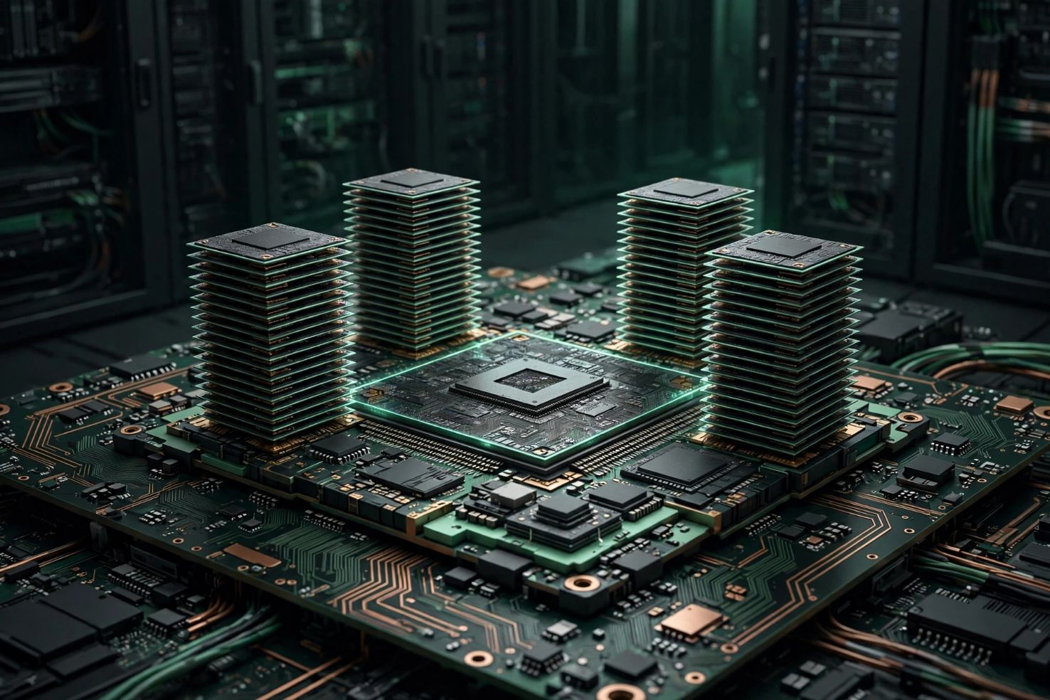
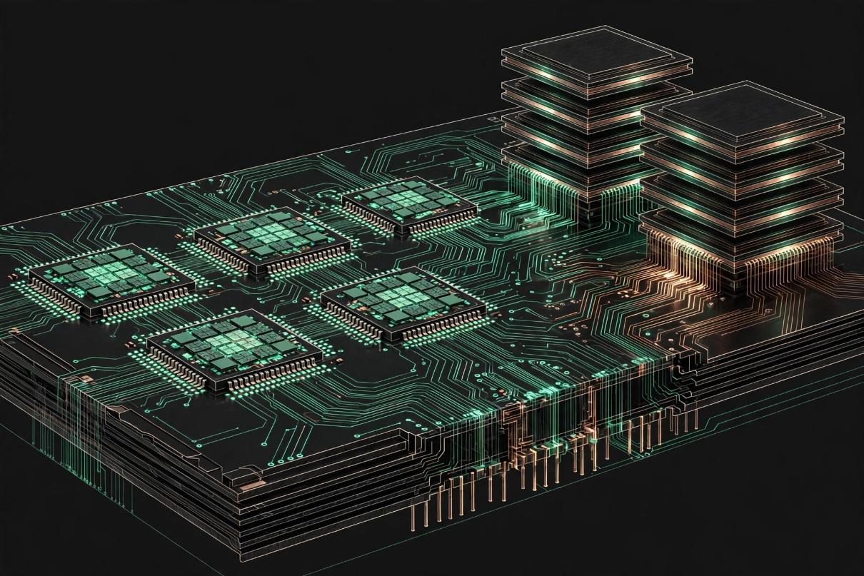
The engineering is a study in pragmatism. Rather than one giant die, the Maia 300 splits into chiplets: the compute tiles are built on TSMC's N2P, a 2-nanometer-class process, while the memory-controller and I/O chiplets use a cheaper 3-nanometer node [4][5]. The logic is straightforward — put the leading-edge silicon only where the math happens, and use older, cheaper processes for everything else [4]. A dedicated device-control chiplet manages power delivery and telemetry, with further chiplets handling data movement in and out of the package [2].[2][4][5]
The generational march is visible in the process nodes alone. The Maia 100 arrived on 5nm in late 2023; the Maia 200 moved to 3nm in January 2026; the Maia 300 now puts its compute on a 2nm-class node [2]. Memory has grown at each step too: 64GB of HBM2E, then 216GB of HBM3E, now 288GB of HBM4 [2]. Three generations in three years is not the pace of a side project — it's the pace of a company that has decided its future runs on its own silicon.[2][4][5]
288 gigabytes of HBM4
If one number explains the Maia 300, it's the memory. Eight stacks of HBM4 deliver 288GB at 18 TB/s of bandwidth, running at 9 Gb/s per pin — roughly a third more capacity and about two and a half times the bandwidth of the Maia 200's 216GB of HBM3E [4][5]. For an inference chip, that ratio matters more than any compute figure: the job is holding enormous models close to the arithmetic, not setting records in raw math.[4][5]
Microsoft's design philosophy is explicit — data movement, not computation, is the main cost in modern inference, so the architecture is built around keeping data close to where it's used [5]. The chip carries 13.8 petaflops of FP4 compute and 6.9 petaflops at FP8, respectable numbers that Microsoft presents almost as an afterthought to the memory system [4][5]. Read it as a memory system with compute attached, rather than the reverse.[4][5]
The 40% claim and its asterisk
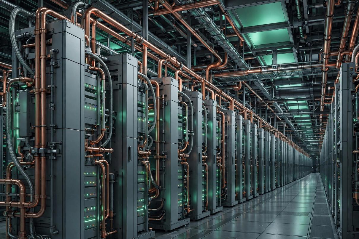
Microsoft's headline efficiency figure is bold: about 40% more useful computing per megawatt than "leading GPU-based systems" [3]. On raw power, each Maia 300 accelerator draws up to 950W — up from the Maia 200's 750W — with 96 of them packed into a single liquid-cooled rack pulling roughly 167 kilowatts, against about 142 kilowatts for NVIDIA's 72-GPU GB300 rack [3][5]. "It's basically delivering more intelligence for every watt, every dollar, and every byte of memory by optimizing across the entire system," Rani Borkar, Microsoft's president of Azure hardware systems and infrastructure, told Reuters [3].[2][3][5]
Now the asterisk, which matters as much as the claim. The 40% figure rests on an unnamed baseline — Microsoft didn't identify the "leading GPU-based systems" it measured against — and no independent testing existed at launch [2]. The previous Maia generation has so far run mostly inside Microsoft's own services, beyond the reach of third-party benchmarks [2]. These are vendor numbers, and TechnoGalaxy treats them as such until silicon meets an independent testbed.[2][3][5]
Superpods and a million chips
The scale of the ambition is arguably the real story. Microsoft stitches 128 racks into "superpods" of 12,288 accelerators — double the 6,144-accelerator clusters of the Maia 200 era — the largest inference fabrics the company has ever assembled [2]. Production deployment begins in 2027, when the Maia 300 is slated to become the primary inference engine across Microsoft's product line [2][4].[2][3][4]
Then there's the volume. A million accelerators at 950W each is, by simple arithmetic, on the order of a gigawatt of power draw — TechnoGalaxy's calculation, not Microsoft's claim — and it signals a bet that owning the silicon beneath inference compounds savings across billions of daily requests [3]. Whether Microsoft hits that number on schedule matters less than what the target reveals: inference at hyperscale has become cheap enough to matter and expensive enough to optimize.[2][3][4]
Broadcom, the arms dealer
If one company sits at the center of the rebellion, it's Broadcom. Days before the Meta announcement, it signed a Long Term Agreement with Google to develop and supply future generations of TPUs, alongside a Supply Assurance Agreement covering networking and other components for Google's next-generation AI racks through 2031 [1]. A year earlier, in October 2025, it announced a co-development deal with OpenAI on custom AI hardware, once targeting deployment in late 2026 and 10 gigawatts of capacity by 2029 [1].[1][6]
Broadcom's earnings call put numbers on the pipeline: a 1.3-gigawatt deployment of Jalapeno — the OpenAI co-developed chip — expected in 2027, a path to 5 gigawatts of TPU shipments for Anthropic, and tens of billions of dollars in processors for Google annually over several years [6]. CEO Hock Tan guided for AI revenue to double to $115 billion in fiscal 2027, then double again to $230 billion in fiscal 2028 [6]. Forecasts are not shipments — but they show exactly where the industry's capital is flowing.[1][6]
Google's decade-long TPU bet
Google is the veteran here — its TPUs have been running production workloads for years — but the new agreements extend the partnership's horizon dramatically. The development agreement covers future TPU generations; the supply assurance pact locks in networking components for next-generation AI racks through 2031 [1]. Broadcom expects the Google relationship alone to be worth tens of billions of dollars in processors annually, including Ironwood TPUs bound for Anthropic's clusters [6].[1][6]
The model differs from Microsoft's go-it-alone approach. Where Maia is a Microsoft architecture fabbed by TSMC, Google's TPUs are co-developed with Broadcom — shared design responsibility rather than a simple foundry transaction [1][6]. Both paths, though, end at the same conclusion: the hyperscalers have decided that renting their AI future entirely from merchant GPU vendors is a strategic risk worth engineering away.[1][6]
OpenAI's Jalapeno
Even OpenAI — the company whose models created the GPU shortage — is designing its way out. Its custom chip, Jalapeno, co-developed with Broadcom, was announced in October 2025 with deployment once targeted for the second half of 2026 [1]. Broadcom now expects a 1.3-gigawatt Jalapeno deployment in 2027, and says OpenAI is already preparing second- and third-generation versions of the silicon [6].[1][6]
The honest caveat first: since the original announcement, neither company has offered substantive public updates on Jalapeno's progress [1]. Roadmaps are not shipments, and a gigawatt of planned deployment is not a gigawatt of running silicon. But the pattern across every major lab — custom programs at Microsoft, Meta, Google, Anthropic, and OpenAI simultaneously — is unmistakable even if any single project slips.[1][6]
Why inference is the prize
Notice what nobody is building: a training chip to dethrone NVIDIA's trainers. Every custom program in this story targets inference — the repetitive, high-volume work of answering prompts [2][4]. The economics explain why. Training a frontier model is a rare, colossal expense; serving it to hundreds of millions of users is a constant, compounding one. When your product answers prompts all day, the chip that answers them cheapest wins the budget.[2][4]
That's the logic Microsoft is betting a million chips on: optimize for tokens per watt and tokens per dollar rather than peak benchmark scores, and let the savings compound across billions of daily requests [2][4]. Inference is also the workload with the most predictable profile — same models, same request shapes, day after day — which makes it the ideal target for fixed-function custom silicon. Training stays general-purpose; serving goes custom.[2][4]
What this doesn't mean
A necessary cooling pass. Every performance figure in this article — the 40%, the petaflops, the gigawatts — comes from the vendors themselves, with no independent verification available at publication time [2][3]. Microsoft's last generation runs inside its own data centers; Meta's MTIA 300 through 500 are future generations on a roadmap; Jalapeno's progress reports have gone quiet [1][2]. Treat the numbers as directionally interesting and specifically unproven.[1][2][3]
And the hyperscalers aren't leaving NVIDIA — they're hedging it. The framing from all parties is "loosening" dependence, not ending it, and the custom chips are consistently positioned as inference systems while training remains GPU territory [2][3]. The rebellion is real, well-funded, and technically serious. It is also, for now, a rebellion of roadmaps and first deployments — not a changing of the guard.[1][2][3]
The bottom line
Pull the week's threads together and the pattern is hard to miss. Microsoft detailed a 2-nanometer chiplet inference chip it plans to deploy by the million; Meta handed its multi-generation silicon roadmap to Broadcom; Broadcom's own numbers revealed a custom-silicon pipeline spanning Google, Anthropic, Meta, and OpenAI [1][2][3][6]. The common thread isn't any single chip — it's the decision, now nearly universal among hyperscalers, that AI's economics demand owning the silicon underneath it.[1][2][3][6]
Whether that silicon is chiplets or monoliths, HBM4 today or denser memory tomorrow, the direction is set: the AI accelerator market is fragmenting from a single-vendor story into a portfolio of custom designs, each tuned to its owner's workloads [1][2]. For the industry, that should mean more competition and, eventually, cheaper intelligence. For NVIDIA, the most interesting threat was never another GPU — it's the customers learning to design their own.[1][2][3][6]
Questions, answered.
What exactly is Microsoft's Maia 300?
A third-generation custom AI inference accelerator unveiled October 12, 2026: compute chiplets on TSMC's 2nm-class N2P process, 288GB of HBM4 at 18 TB/s, 13.8 petaflops of FP4 compute, 950W per chip, with production deployment starting 2027 [2][4].[2][4]
What did Meta and Broadcom agree to?
A multi-generation co-development partnership for Meta's MTIA chips — design, advanced packaging and networking on Broadcom's XPU platform — with an initial commitment above a gigawatt of compute; Broadcom CEO Hock Tan moves from Meta's board to an advisory role on the silicon roadmap [1][6].[1][6]
Does this mean NVIDIA is finished?
No. All figures are vendor-reported, most deployment is in the future, and the hyperscalers frame this as loosening dependence for inference — training remains GPU territory [2][3].[2][3]
Read the sources.
- Meta partners with Broadcom for development of "multiple generations" of MTIA chipsData Center Dynamics · Accessed 2026-10-24
- Microsoft Maia 300 Chip Bets on Power and Memory, Not SpeedMemeburn · Accessed 2026-10-24
- Microsoft plans huge deployment of its own AI chips, with an eye on saving costsReuters · Accessed 2026-10-24
- Microsoft's Maia 300 Is Its Biggest Bet on Its Own Silicon: 288 GB of HBM4, 2nm Chiplets, and 40% More Tokens per MegawattTech Featured · Accessed 2026-10-24
- Microsoft unveils Maia 300 custom AI inference chipRCR Tech · Accessed 2026-10-24
- Broadcom delivers strong earnings view as CEO touts growth with AI labsRocketNews · Accessed 2026-10-24
Contributor articles and source links do not guarantee error-free reporting. See our editorial policy.